Navigation

    MakerGram Logo

    MakerGram

    • Register
    • Login
    • Search
    • Categories
    • Recent
    • Popular
    • Tags
    • Users
    • Groups

    PCB Design for ESP32 Stand alone module

    PCB Designing
    esp32 pcb
    6
    30
    5390
    Loading More Posts
    • Oldest to Newest
    • Newest to Oldest
    • Most Votes
    Reply
    • Reply as topic
    Log in to reply
    This topic has been deleted. Only users with topic management privileges can see it.
    • kowshik1729
      kowshik1729 last edited by kowshik1729

      @Sharmila GPIO0 must not be low all the time. It must be held low only for a moment. Because GPIO0 is a boot strap option for choosing between UART download and normal operation. Please refer to the datasheet and search boot strap. And also can you please post a snap of your newly designed board please?

      S 2 Replies Last reply Reply Quote 1
      • S
        Sharmila @kowshik1729 last edited by Sharmila

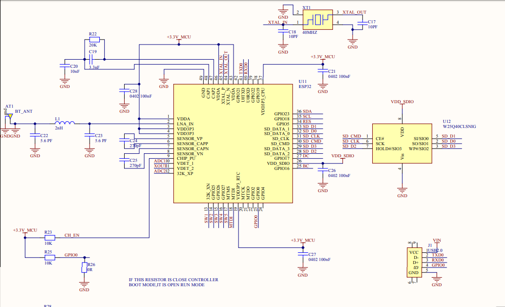
        @kowshik1729 thank you for the hint ! i will check it . schematic picture of my board is given below

        (freesnippingtool.com_capture_20200721122206.png)

        1 Reply Last reply Reply Quote 1
        • S
          Sharmila @kowshik1729 last edited by

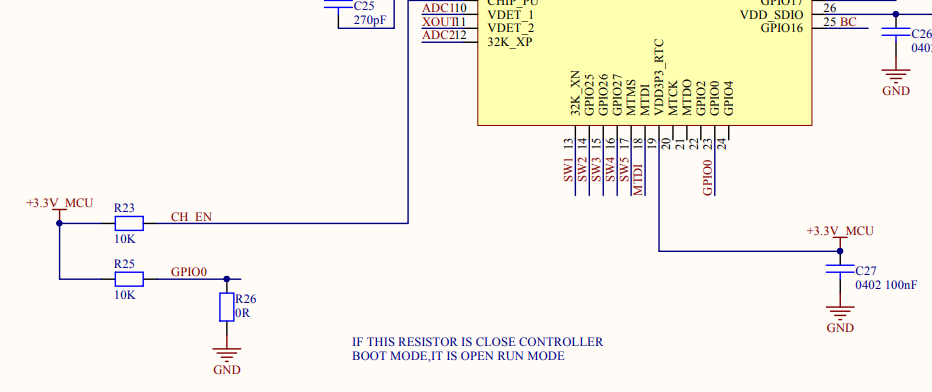
          @kowshik1729 sorry, gpio 0 is low only till it is programmed. after that this will disconnected.

          1 Reply Last reply Reply Quote 0
          • kowshik1729
            kowshik1729 last edited by

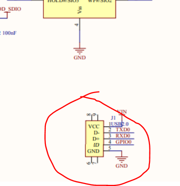
            @Sharmila Reviewed your schematics. Have the following doubts

            1. Is this a USB receptacle?

            4f585013-72f9-4ceb-bc72-8fa40ff32a36-image.png

            1. Didn't find any option where you can pull the GPIO0 low and bring it back to normal state. Did you have a jumper connection or button between GPIO0 and GND?
            1 Reply Last reply Reply Quote 0
            • S
              Sharmila last edited by

              1. no.
              2. we are using jumper for gpio 0th pin. please refer the below image.
                freesnippingtool.com_capture_20200721200934.png
              1 Reply Last reply Reply Quote 0
              • First post
                Last post

              Recent Posts

              • Hi all,

                I recently came across this post where they have shown photos printed on PCB in high resolution. I would like to know how to add this kind of photos to the silkscreen layers of the PCB in Eagle/Altium.

                Adding such kind of photos will be attractive for beginners and also can be used for educational purposes too.
                Please let me know in case anybody knows.

                • read more
              • @kowshik1729 I think that might not get since the platform is not opensource! but they provided everything you need to develop a system with that.

                • read more
              • @kowshik1729 Carrier board schematics for SoMs will be always available as they need to be modified as per customer application, however SoM design files are hard to get unless the H/W design is truly open-source.

                • read more
              • @salmanfaris Actually the schematics files you've mentioned are the same files which I've got from them. They are carrier board design files.😢

                • read more
              • @kowshik1729 Please check this, it might help you,

                Jetson Nano Module Datasheet Jetson Nano Product Design Guide Jetson Nano Thermal Design Guide Jetson Nano 3D CAD STEP Model Jetson Nano Developer Kit 3D CAD STEP Model Jetson Nano Pinmux Table Jetson Nano Developer Kit Pinmux Table Jetson Nano Reference Design Schematics More resource

                originally drafted and shared by dusty_nv

                • read more
              By MakerGram | A XiStart Initiative | Built with ♥ NodeBB
              Copyright © 2020 MakerGram, All rights reserved.
              Privacy Policy | Terms & Conditions | Disclaimer | Code of Conduct