That's alright @kowshik1729 i will check other forum and also await your answer. also i am trying to calculate the pcb track width and via diameter for the board, i am asking since we printing similar boards.
Thanks....
Posts made by ZeeZa
-
RE: Schematic Design For esp32posted in PCB Designing
-
RE: Schematic Design For esp32posted in PCB Designing
Thanks for your amazing explanations... but still not done yet
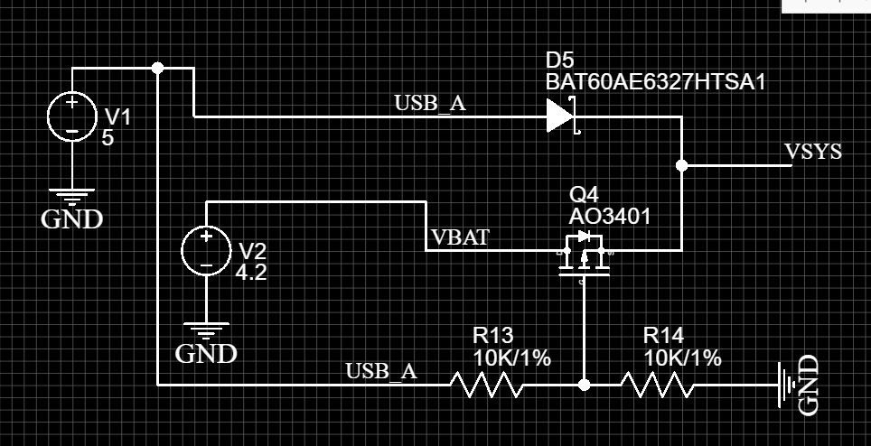
i have this power switching circuit

i have a little doubt about the mosfet in the circuit basically when there is a voltage in the V1(5v) it gets divided before going to the gate then the gate turns on the mosfet that is the USB(V1) power is used by the device, what i dont understand is the VBAT(V2) should be connect to the drain or source of the mosfet, i think it should be the source but there is a diode between the drain and the source which will be forward bias if current is flowing from the drain(I might be wrong), which mean current wont flow from source to the drain.
-
RE: Schematic Design For esp32posted in PCB Designing
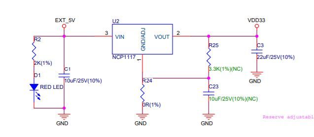
Thanks for your kind explanations, but in that circuit it already have an input EXT_5V capacitor C1 which is 10uF and a output of 22uF at c3 before going to power VDD33, my question here is the R25 resistor and R24(what does 0R even mean) and C23 capacitor are they really needed in the circuit? i mean if like you said every ic on a pcb board take little bit of power so why populate it with unnecessary resistors and capacitors. and also how can i simulate this link text circuit, i am still looking for simulation mode on easyeda for the past 2 days... still looking...
Thanks... -
RE: Schematic Design For esp32posted in PCB Designing
thanks for the answers @kowshik1729 but before you answer the remaining question i have some few more,

in this schematic 3.3K(1%)(NC) and 10uF/25V(10%)(NC) i assume that they do not need to be connected, Is that correct? -
RE: Schematic Design For esp32posted in PCB Designing
@kowshik1729
I'm still on the pcb design, can you check link text and give a feedback(the pcb wring) and also do i have to worry about unest pins and final question do the usb to uart ic consume power when i connect the device to a battery power? still not decided over uart and jtag yet..
Thanks.. -
RE: Schematic Design For esp32posted in PCB Designing
@kowshik1729
i tried the link you gave and i don't have most of the components they used especially the ESP32-S so i tried improvising, i used the arduino and DOIT ESP32 DEVKIT V1, i can't upload to my DOIT board cause the USB port got damaged so i tried connect to arduino the same way they connect to the FDTI in the circuit, i didnt border about the buttons cause it is already on the DOIT board.
After all the connections, when i tried uploading i was not able to connect to the DOIT board i got "
A fatal error occurred: Failed to connect to ESP32: Invalid head of packet (0x0A)"
I tried holding the boot button down also but got the same error. -
RE: PCB Design for ESP32 Stand alone moduleposted in PCB Designing
@salmanfaris
i tried uploading a code to the Esp32 by connecting to arduino with the connection below
Arduino Tx to ESP32 Tx0Arduino Rx to ESP32 Rx0
Arduino 3v3 to ESP32 3v3
Gnd to Gnd
And connecting Arduino Reset Pin to ground....
I could read the esp32 from the serial monitor but the code is not getting uploaded to the board(esp32).. I am trying this method so that if it works i wont have to add Jtag or USBtoUART on my pcb..
Thanks.. -
RE: Schematic Design For esp32posted in PCB Designing
am sorry if i am asking some basic question i still cant get my head wrap around the JTAG pins, let say i have the JTAG in my pcb how will i use the pin to program the device from my Laptop(IDE) or is the Jtag used the same way we use the ESP-01 which we connect to Arduino UNO rx and tx pin before we can upload the code on it?
-
RE: Schematic Design For esp32posted in PCB Designing
@kowshik1729 said in Schematic Design For esp32:
JTAG connections
i am trying to make the pcb as slim as possible here and adding the jumper will make it a little bigger width wise, i thought the the UART(JP1) is for uploading the code to the esp module as it is connected to TXDO and RXDO or is it only serving as a power connect in this schematic?
-
RE: Schematic Design For esp32posted in PCB Designing
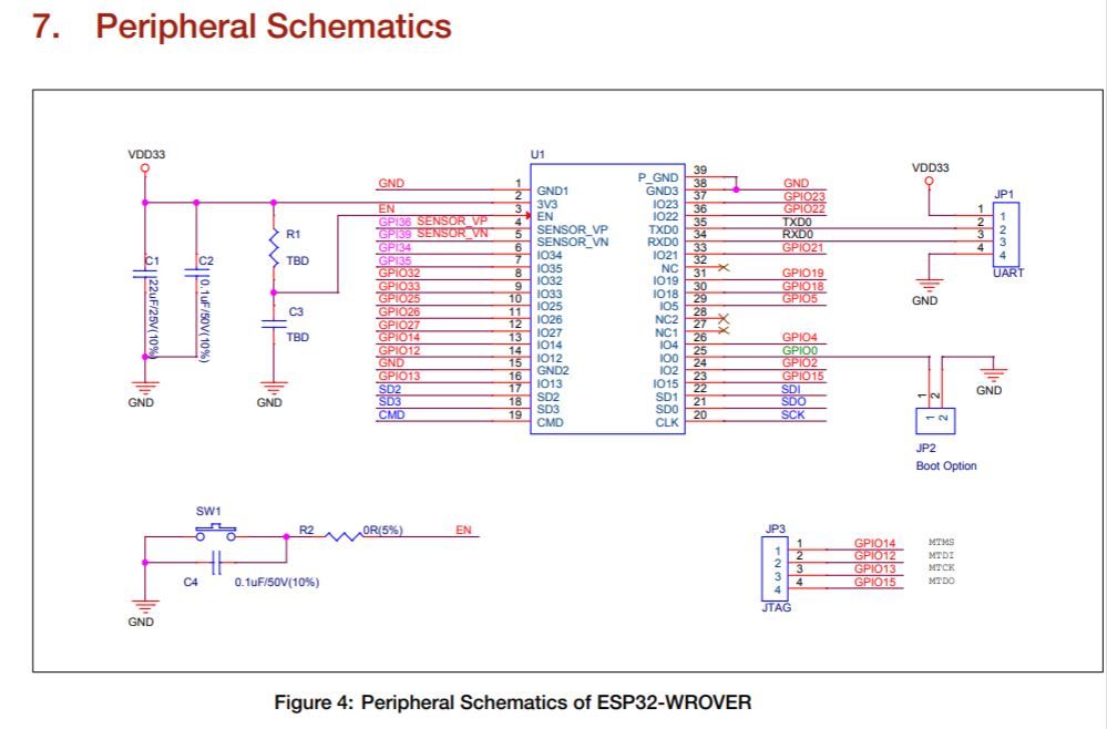
Thanks for the replies.. so far i have been able to achieve this link text but i am having so doubts when following the datasheet of link text page 15 here is the image
 , I do not understand what the JP3(Jtage) is for, can someone please explain, also i have this other link link text he did the same thing am doing but way more than mine. so i am following some of his schematics. also i have a lot of unfinished net in my schematic please how do i deal with them... Thanks