Schematic Design For esp32
-
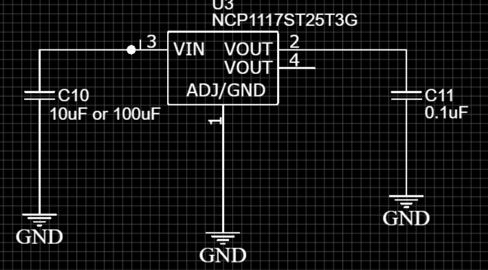
Thanks for your kind explanations, but in that circuit it already have an input EXT_5V capacitor C1 which is 10uF and a output of 22uF at c3 before going to power VDD33, my question here is the R25 resistor and R24(what does 0R even mean) and C23 capacitor are they really needed in the circuit? i mean if like you said every ic on a pcb board take little bit of power so why populate it with unnecessary resistors and capacitors. and also how can i simulate this link text circuit, i am still looking for simulation mode on easyeda for the past 2 days... still looking...
Thanks... -
@ZeeZa Regarding the 0R resistor, it means that the value of resistance is ZERO it acts as a virtual short path by providing little rugged path than a normal copper wire. The main use of this 0R resistances is that it gives stable transients at output and input terminals. But it is redundant, meaning you need not necessarily include it in your schematics always. C23 and R25 can also be skipped. So, by consolidating all the above changes the final schematic can be something like this
For simulation part, you don't have to necessarily use only easy EDA, you can use softwares like Proteus or Fritzing like that. -
Thanks for your amazing explanations... but still not done yet
i have this power switching circuit
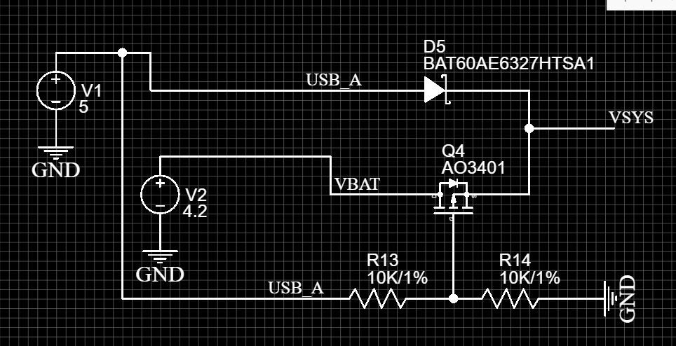
i have a little doubt about the mosfet in the circuit basically when there is a voltage in the V1(5v) it gets divided before going to the gate then the gate turns on the mosfet that is the USB(V1) power is used by the device, what i dont understand is the VBAT(V2) should be connect to the drain or source of the mosfet, i think it should be the source but there is a diode between the drain and the source which will be forward bias if current is flowing from the drain(I might be wrong), which mean current wont flow from source to the drain.
-
@ZeeZa I'm really really sorry that I couldn't help you with this question alone. Because I'm really not that good regarding the MOSFET's thing but I can answer if you could afford me some time. Sorry about that.
-
That's alright @kowshik1729 i will check other forum and also await your answer. also i am trying to calculate the pcb track width and via diameter for the board, i am asking since we printing similar boards.
Thanks....
Recent Posts
-

Hi all,
I recently came across this post where they have shown photos printed on PCB in high resolution. I would like to know how to add this kind of photos to the silkscreen layers of the PCB in Eagle/Altium.
Adding such kind of photos will be attractive for beginners and also can be used for educational purposes too.
Please let me know in case anybody knows. -

@kowshik1729 I think that might not get since the platform is not opensource! but they provided everything you need to develop a system with that.
-

@kowshik1729 Carrier board schematics for SoMs will be always available as they need to be modified as per customer application, however SoM design files are hard to get unless the H/W design is truly open-source.
-
@salmanfaris Actually the schematics files you've mentioned are the same files which I've got from them. They are carrier board design files.
