Schematic Design For esp32
-
Hello guys
I want to create a schematic design for a esp32 module with MPU6050 chip as well as a battery connector and a battery charger, it is similar to link text but i want to use the esp32 module not the chip.. i have already achieve this using the esp32 dev board and MPU6050 board and a battery charger as per the picture below(couldn't attach a zip file) but the issue is the battery consumption is very high and the size is very big also...
This will be my first time trying to make my own device(Schematic) i am good using the boards and connecting them but not joining ICs on a PCB.. please any help on how to achieve this will be welcomed.. -
Hi @ZeeZa ,
You need to build a custom board with the ESP32 SoC and the MPU6050 IMU, right?
first, you need to select appropriate ESP32 SoC from the wide variety of model, after that using the datasheet find out the minimum configuration circuit for the SoC and add the MPU6050 module. that's all you need. the most tricky part is the minimum configuration circuit.
-
@ZeeZa I'm working on a similar type of project. As @salmanfaris has mentioned the minimum config of ESP32 is important. But, If you are trying to use the SoC versions like ESP32 WROVER then you can directly interface it with MPU6050 IC. If you're trying to use bare IC instead of the breakout board of the MPU6050 then I suggest you see this link which will give you the configuration to be made for the MPU6050 IC to interface with your MCU.
I suggest you to even look at the datasheet of the ESP32 because they have mentioned how you must place the SoC module on PCB. You cannot place the module in the middle of the board as it causes bad reach to the antenna. The SoC must be placed at the edges of the PCB with antenna side protruding outside. There are many other design rules mentioned in the datasheet. So, Please refer it before you start your work. All the best, happy making..!!

-
Thanks for the replies.. so far i have been able to achieve this link text but i am having so doubts when following the datasheet of link text page 15 here is the image
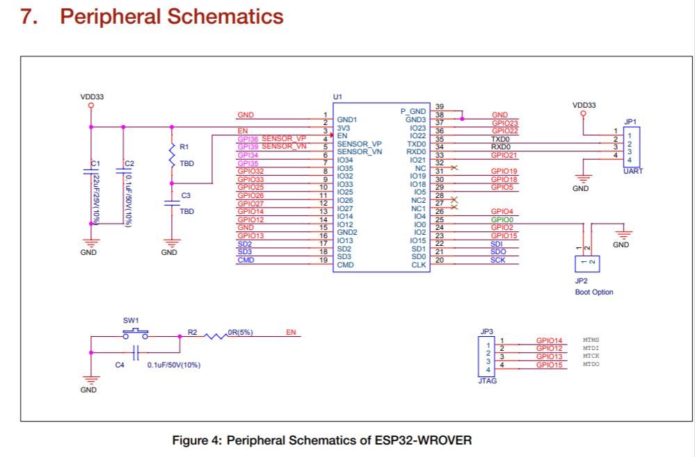 , I do not understand what the JP3(Jtage) is for, can someone please explain, also i have this other link link text he did the same thing am doing but way more than mine. so i am following some of his schematics. also i have a lot of unfinished net in my schematic please how do i deal with them... Thanks
 -
@ZeeZa JP3 in the schematic means Jumper slots for JTAG connections. jtag is nothing but an IEEE standard used for programming and debugging the microcontrollers. It is more sophisticated than other protocols so far. So, In order to program your MCU with the code that you write on your IDE, we need these pins for burning the code. You can even burn the code in prior and populate the SoC onto your PCB. But, it's more recommended to make these JTAG connections so that you can program it whenever you wanted.
-
@kowshik1729 said in Schematic Design For esp32:
JTAG connections
i am trying to make the pcb as slim as possible here and adding the jumper will make it a little bigger width wise, i thought the the UART(JP1) is for uploading the code to the esp module as it is connected to TXDO and RXDO or is it only serving as a power connect in this schematic?
-
@ZeeZa The JP1 UART jumper doesn't serve as the power connect. It is meant for extending the UART pins so that you can access them. JTAG is responsible for uploading the code and I understand that you are not ready to compromise over the size of PCB. So, I suggest you use CP2102 USB to UART converter where you can just connect your mini USB cable and upload the code. This is even easier, but if you see the ESP32 development module, it is just the same board where ESP32 SoC is fit which can be accessed with a USB to UART converter.
You can use these
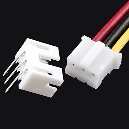
for extending the JTAG pins. These are a little small and can reduce the width of the PCB. Please let us know in case of queries. You ca easily find the footprints of these connectors in your PCB designing softwares.
-
am sorry if i am asking some basic question i still cant get my head wrap around the JTAG pins, let say i have the JTAG in my pcb how will i use the pin to program the device from my Laptop(IDE) or is the Jtag used the same way we use the ESP-01 which we connect to Arduino UNO rx and tx pin before we can upload the code on it?
-
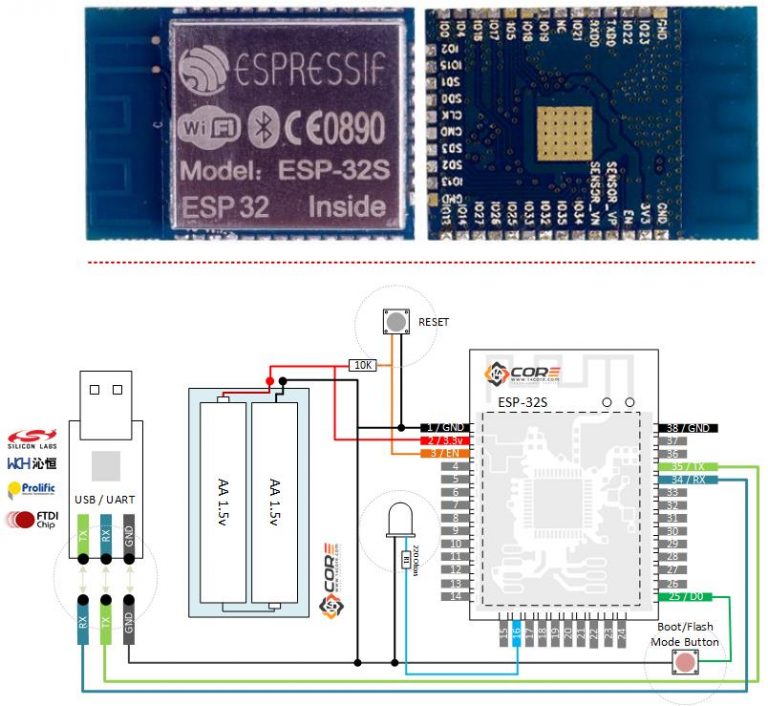
@ZeeZa JTAG Programmer for ESP32
You can programme your board using the JTAG pins on your PCB by connecting them to the JTAG pins of the programmer board.
-
@ZeeZa Have you figured out a way how to programme your ESP32 using UART pins?? If not Well, I did found out a way. please this link ESP32 UART UPLOAD
May be this might help you out..!! Please try out and let me know your output.
Recent Posts
-

Hi all,
I recently came across this post where they have shown photos printed on PCB in high resolution. I would like to know how to add this kind of photos to the silkscreen layers of the PCB in Eagle/Altium.
Adding such kind of photos will be attractive for beginners and also can be used for educational purposes too.
Please let me know in case anybody knows. -

@kowshik1729 I think that might not get since the platform is not opensource! but they provided everything you need to develop a system with that.
-

@kowshik1729 Carrier board schematics for SoMs will be always available as they need to be modified as per customer application, however SoM design files are hard to get unless the H/W design is truly open-source.
-
@salmanfaris Actually the schematics files you've mentioned are the same files which I've got from them. They are carrier board design files.
