Custom PCB Shapes using Eagle
-
Hello,
I'm working on a PCB design that uses ESP32 processor. I want to make a custom PCB shape using Eagle(It's by default an arbitrary rectangle in eagle though). How can i make different shapes like circle, Hexagon or any custom PCB shape? Is it possible with Trail version of Eagle ? -
Hi @kowshik1729,
Yes, you can import the .dxf drawings file to PCB Board design, but I recommend is that use Autodesk Fusion360, you can collaborate with eagle .
Step 1: Create Fusion360 design
Step 2: Select Creat PCB from Creat -> Create PCB
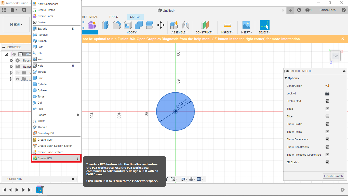
Step 3: Click Create PCB Profile
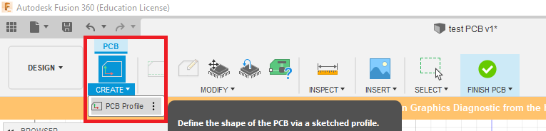
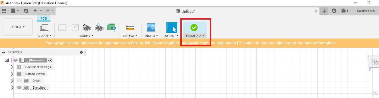
Step 4: Click Finish PCB and Save to Fusion
Step 5: Open Eagle and Sign with the same account that used Fusion360
Step 6: Open Board Design file and Select Fusion360 Icon on the right side and Select Option One that links to existing fusion design
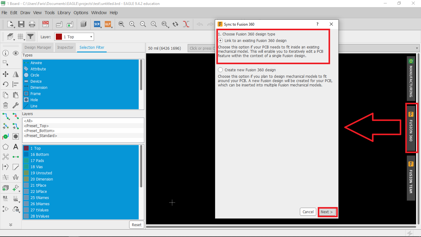
Step 7: Select Fusion Project from the following project list and select the PCB file
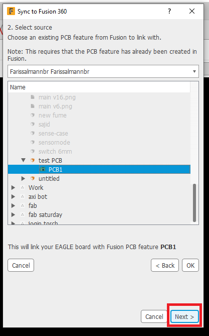
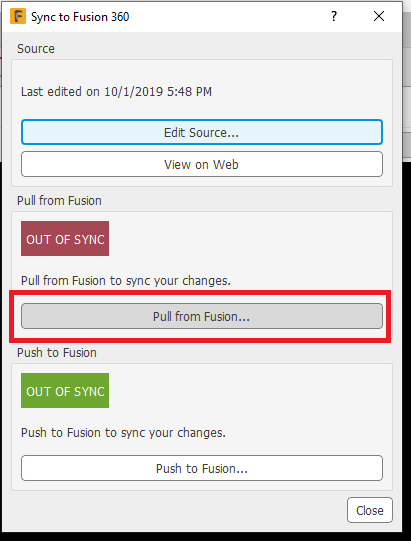
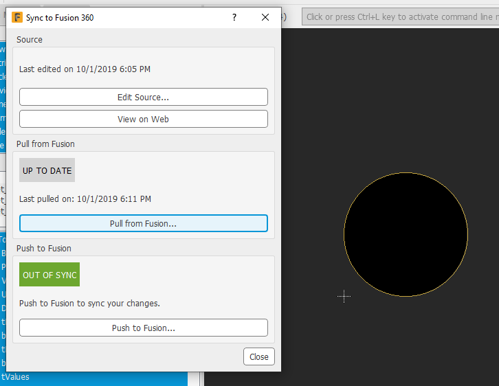
Step 8: Click Pull From Fusion to Sync the design with Eagle
Step 9: If everything done perfectly you can see the PCB board outline in eagle
All the best
-
@salmanfaris Woow, thank you soo much. This is very explanatory...!!
Recent Posts
-

Hi all,
I recently came across this post where they have shown photos printed on PCB in high resolution. I would like to know how to add this kind of photos to the silkscreen layers of the PCB in Eagle/Altium.
Adding such kind of photos will be attractive for beginners and also can be used for educational purposes too.
Please let me know in case anybody knows. -

@kowshik1729 I think that might not get since the platform is not opensource! but they provided everything you need to develop a system with that.
-

@kowshik1729 Carrier board schematics for SoMs will be always available as they need to be modified as per customer application, however SoM design files are hard to get unless the H/W design is truly open-source.
-
@salmanfaris Actually the schematics files you've mentioned are the same files which I've got from them. They are carrier board design files.
