Need Help: ESP32 PICO Antenna Design
-
For this, you need 50 ohm impedance feed line.
-
Dear @kowshik1729 & @salmanfaris
Antenna designing is a little bit complicated because a lot of parameters affect the antenna's performance. i briefly explain what i know and if you guys still have doubts then shoot me.Even if you use any type of antenna we need to do the impedance matching. If your application only has RX then you don't really need the impedance matching network. But if you have RX/TX part then you should need an impedance matching network in between the source and load (feed line).
The impedance matching network is used to keep the 50 Ohms(depends) impedance while receiving or transmitting through the source and load. If there is an unmatched matching network there is high-performance dropping and also it will affect the RF chip life. Assume If there is no matching network then there is a high chance for reflection back to the chip while doing transmitting. This will affect the chip to heat up quickly and gradually damage the chip.
To do the matching network is not that easy(in my case). The RF chip doesn't have much role in this part. We can find a few information like how much impedance we need to keep and related etc...
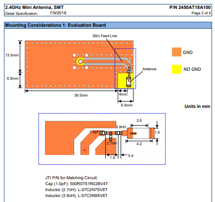
and in Antenna's datasheet, we could find information regarding ground clearance feed line, etc...
the information shows in the antenna datasheet like @salmanfaris shared recently, it is an evaluation board to show an example where we need to place the chip, clearance of the chip and how we need to place the chip, etc...But the matching network they used in the evaluation board is just for that board. Your design will be different from that board like you have a lot of components on the board the shape of the board and the ground stitching etc... will affect your matching network. The matching network type does not matter you can use any type like PI, L, T etc.... but the values will be changed depends on the PCB design. To tune the matching network you need to use a vector analyzer device to measure the performance of the matching network and if it unmatched then you can calculate the values of the Inductor and capacitors by tweaking the values in the SMITH CHART.
if your design is just for hobby purpose it doesn't really matter because even a coil will act as an antenna(have a lot of cons but it do the job). But if your purpose is to sell or share or you are concerned about the life of the device then you need to do tune the matching network. In my case, I am concerned about both cases.
It is best to sue the chip antenna rather than a trace antenna because of performance. but all chip antenna will not bring that performance. For example, the Rainsun antennas are cheap but they only give the performance like a trace antenna gives you. but if you are concerned about the shape and size of the board, it will help you a lot. I recommend JOHANSON antennas they are cheap and give much better performance. But it still a 2D antenna. If you can afford a 3D antenna i recommend antennas from FRACTUS antennas or Proant AB antennas. But they are really expensive but they have good performance in the case of range and low noise.
Let me know if you guys need to know anything more or i miss anything
")
-
@Suhailjr Woow....Firstly I thank you very much for your patience to explain me very elaboratively. Yeah I have read many articles (in fact referred some books too) regarding my RF layout. The issue I was having here is, instead of having the impedance matching circuitry, I wanna implement a microstrip line which will eliminate the requirement of any external devices like caps and inductors. I do not have VNA kinda equipment to test it....So I need a workaround to directly implement on my board.
I have previously made a design with this antenna by contacting the Johanson Technology Application Engineer's team. We have made a layout with impedance matching circuitry but that board was a mere waste. I did not design the board any where near to RF layout guidelines. It's just a two layer board with pretty messed up components placement.
So, I decided to properly make this board with 4 layers with the stack divided as following
Top -> RF Layer
Second -> GND Plane (Microstrip line will be designed with reference to this)
Third -> VCC Plane
Bottom-> Signal LayerLet me know if you have designed any boards with microstrip lines. That would be a great help to me....!!
-
Hi Did you got assistance regarding antenna design
-
@naveenDesign Me and @Suhailjr are still working on the designing part. Please put up your thoughts if any, we are glad to know.

Recent Posts
-

Hi all,
I recently came across this post where they have shown photos printed on PCB in high resolution. I would like to know how to add this kind of photos to the silkscreen layers of the PCB in Eagle/Altium.
Adding such kind of photos will be attractive for beginners and also can be used for educational purposes too.
Please let me know in case anybody knows. -

@kowshik1729 I think that might not get since the platform is not opensource! but they provided everything you need to develop a system with that.
-

@kowshik1729 Carrier board schematics for SoMs will be always available as they need to be modified as per customer application, however SoM design files are hard to get unless the H/W design is truly open-source.
-
@salmanfaris Actually the schematics files you've mentioned are the same files which I've got from them. They are carrier board design files.
