Day 1: Introduction To Printed Circuits Boards
-
Overview
One of the key concepts in electronics is the printed circuit board or PCB. It's so fundamental that people often forget to explain what a PCB is. This tutorial will breakdown what makes up a PCB and some of the common terms used in the PCB world.
Here we are using Sparkfun PCB Basic tutorials, and after that, we have some ToDO that you need to complete.
Resource Link: https://learn.sparkfun.com/tutorials/pcb-basics/all
ToDo:
- Find the Annular ring, Drill hit, Finger, Mouse bites, Pad, Silkscreen, Slot on the PCB you used (ex: Arduino Uno, Relay) and Document it (Docs, Github, MakerGram..etc)
- List out PCB designing Softwares
- Download and Install Autodesk Eagle
-
can you please explain it again on why those gaps were made at the bottom of relay boards??
-
Hi @jerin_peter ,
The answer to your question is “isolation”. When designing electronics products involving more than one type of signal or more than one operating voltage, isolation is used to prevent one signal from messing up the other. It also plays a vital role in safety by preventing fault conditions in industrial-grade products. This isolation is generally referred as Galvanic isolation.
In the relay, we are using Power isolation and it's are required to isolate low power-sensitive devices from high power noisy lines or vice versa. Also, power level isolation provides proper safety from hazardous line voltages by isolating the high voltage lines from the operator and other parts of the system.
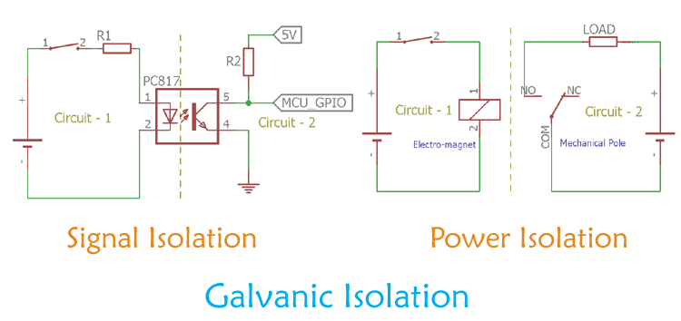
img src: circuitdigest -
@salmanfaris Ohhh Thankyou sir, Well explained


Recent Posts
-

@Ggreeshma-stani Pretty good than the previous design. I am able to see 2 crystals on the board. Can I know why did you use another one?
And finally, you can address me as kowshik. No need of sir

-
@hisham Ahaaa...!! Looks like you've fixed the error. Great job.
We'll be glad to have a look once your PCB is fabricated...
-

@hisham also make sure Design Rules are matching with our manufacture capabilities! In this case, we are planned to use Seeed Studio Fusion PCB Service, so you can check their PCB capabilities and configure your PCB Design Rules.
Fusion PCB Specification