Day 3: Create Board layout from Schematics
-
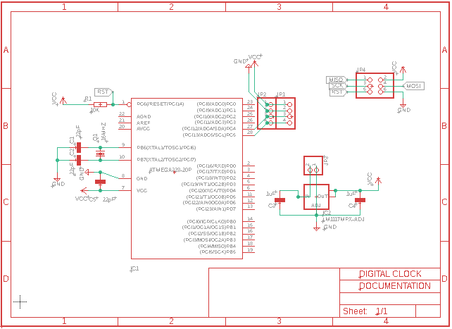
Yesterday we created the DigitalClock Schematics and today we are convert the Schematics into Board layout and complete the PCB Design.
ToDo:
-
Design your own board from your Schematics file
-
Document and share here.
-
-
-
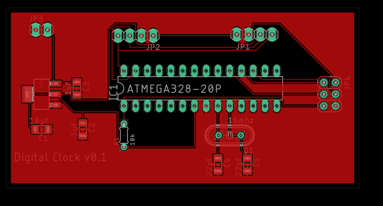
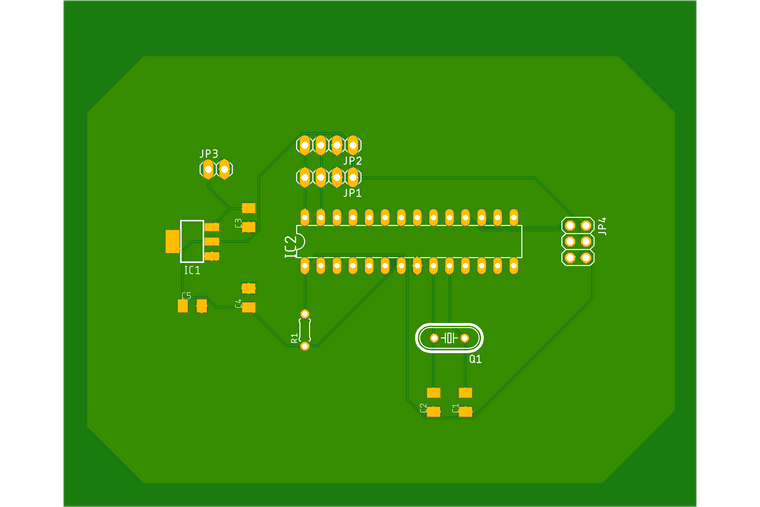
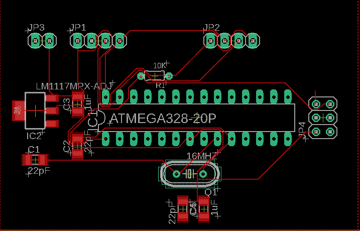
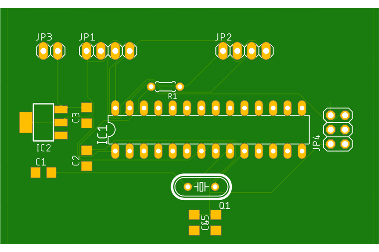
Created board layout for Atmega based digital clock on attending the online workshop on Autodesk Eagle by @salmanfaris .
-
PCB DESIGN DIGITAL CLOCK
SIMPLE LED
-
Created board layout for Atmega based digital clock on attending the online workshop on Autodesk Eagle
Recent Posts
-

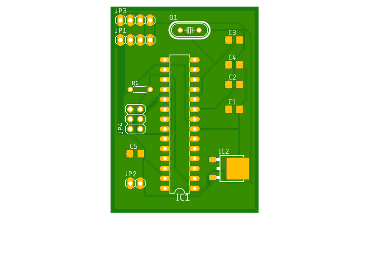
@Ggreeshma-stani Pretty good than the previous design. I am able to see 2 crystals on the board. Can I know why did you use another one?
And finally, you can address me as kowshik. No need of sir

-
@hisham Ahaaa...!! Looks like you've fixed the error. Great job.
We'll be glad to have a look once your PCB is fabricated...
-

@hisham also make sure Design Rules are matching with our manufacture capabilities! In this case, we are planned to use Seeed Studio Fusion PCB Service, so you can check their PCB capabilities and configure your PCB Design Rules.
Fusion PCB Specification